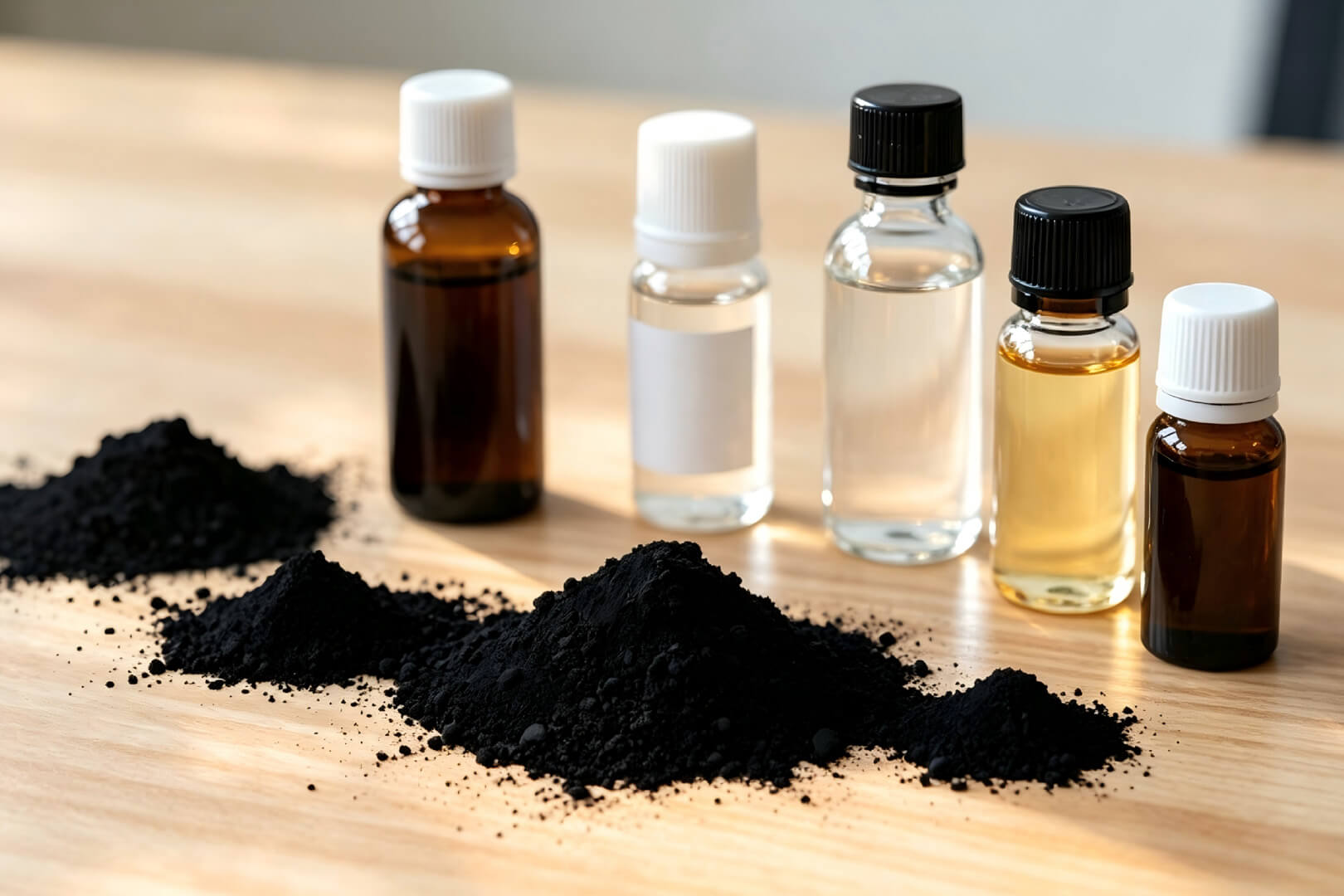
A crystalline solar wafer needs 130–200 micrometers of silicon to do its job. A thin-film device does the same physics with one or two — because amorphous silicon absorbs sunlight about a hundred times more strongly than its crystalline cousin, with an absorption coefficient near 10⁵ cm⁻¹ and a bandgap around 1.7 eV. That hundredfold difference is the entire promise of thin-film silicon: the same element, the same non-toxic abundance, deposited as a coating measured in nanometers rather than a slice measured in millimeters.
Eata Silicon supplies the thin-film silicon materials that research laboratories and industrial coating operations work with: high-purity silicon sputtering targets, amorphous and microcrystalline silicon coatings on glass and flexible substrates, and characterized test coupons for process development.
Browse Our Products
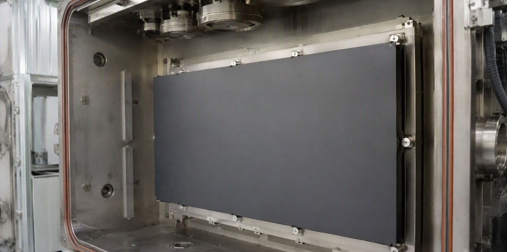 A silicon sputtering target mounted in a coating line.
What Thin-Film Silicon Is — and Why It Still Matters
Deposit silicon from a vapor at low temperature and it freezes without long-range order: that is amorphous silicon, and once its dangling bonds are passivated with hydrogen it becomes device-grade a-Si:H. Push the process toward higher hydrogen dilution and nanometer-sized crystals begin to form inside the amorphous matrix — that is microcrystalline silicon, µc-Si:H, which keeps a 1.1 eV bandgap and reaches far into the near-infrared. Both can be doped n-type or p-type during growth simply by adding phosphine or diborane to the gas mixture, and both coat glass, metal foil, or plastic with equal ease.
The technology is older than most of today's solar industry — it powered calculators in the 1980s and still builds the transistor backplane of every LCD screen — yet it keeps finding new work: indoor energy harvesting for IoT devices, semi-transparent building glass, flexible power sheets, and the carrier-selective layers inside the record-breaking tandem cells now dominating photovoltaic research.
How the Films Are Made
- PECVD: the workhorse route — silane diluted in hydrogen decomposes in a radio-frequency plasma at around 200 °C, growing uniform a-Si:H or µc-Si:H over large areas at low temperature.
- VHF-PECVD: driving the plasma at very high frequency raises deposition rates without sacrificing material quality, the standard answer for thicker microcrystalline absorbers.
- Hot-wire CVD: silane cracks thermally on filaments above 1,500 °C — no ion bombardment, excellent gas utilization, and gentle conditions for sensitive substrates.
- Magnetron sputtering: the physical route, where argon ions blast silicon atoms off a solid target — no process gas chemistry at all, which is why our sputtering targets serve coating lines from research chambers to architectural glass.
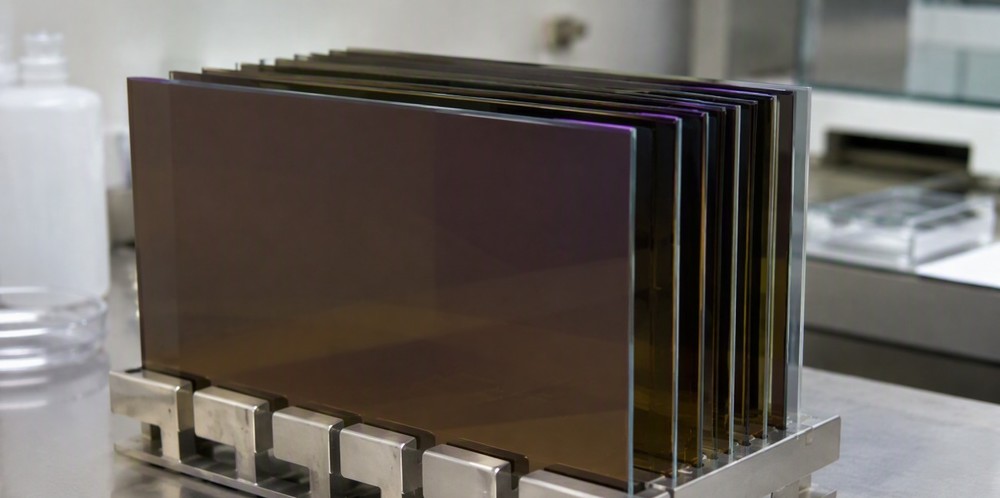 Amorphous-silicon-coated glass panels in the lab.
Where Thin-Film Silicon Works Best
- Indoor photovoltaics and IoT power: under LED lighting a-Si cells convert up to about 21%, versus only 4–6% for crystalline silicon — the reason sensors, remote controls, and shelf labels run on thin-film strips.
- Building-integrated photovoltaics: semi-transparent a-Si glass delivers a perfectly uniform facade appearance with no visible cell grid, while generating power from daylight.
- Flexible and lightweight PV: films on polyimide or metal foil bend, roll, and weigh almost nothing — suited to curved surfaces, portable power, and roll-to-roll production.
- Display electronics: the a-Si:H thin-film transistor remains the switching element behind flat-panel screens worldwide.
- Tandem and heterojunction research: micromorph a-Si/µc-Si stacks, and the ultra-thin doped silicon layers that make silicon heterojunction and perovskite-silicon tandem cells possible.
- Photosensors and detectors: large-area PIN photodiodes and imaging arrays built on the same material platform.
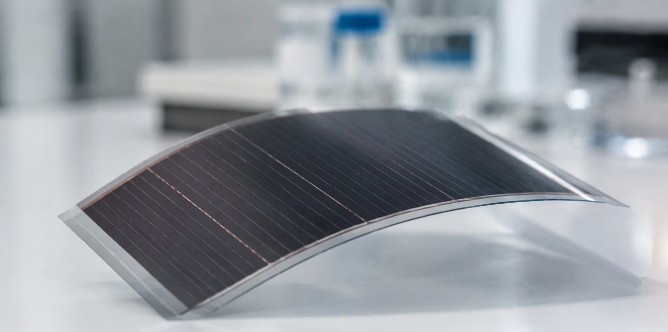 A flexible thin-film silicon strip on a polymer substrate.
Amorphous, Microcrystalline, or Micromorph?
Three material forms cover three slices of the spectrum. Choosing between them — or stacking them — is the first decision in any thin-film project:
| Material |
Bandgap |
Strengths and Record Performance |
| a-Si:H (amorphous) |
~1.7 eV |
Strong visible-light absorption, excellent low-light response; stabilized single-junction record about 10% |
| µc-Si:H (microcrystalline) |
~1.1 eV |
Absorbs beyond 1,000 nm into the infrared; stable against light-induced degradation |
| Micromorph tandem (a-Si / µc-Si) |
1.7 + 1.1 eV |
Two stacked cells share the spectrum; confirmed stabilized record 11.7%, modules around 9% |
One honest caveat belongs here: amorphous silicon loses some performance in its first weeks of light exposure — the Staebler-Wronski effect — before stabilizing. Good device design, thin intrinsic layers, and tandem architectures keep the stabilized figures respectable, and all our a-Si:H materials are specified at their stabilized values.
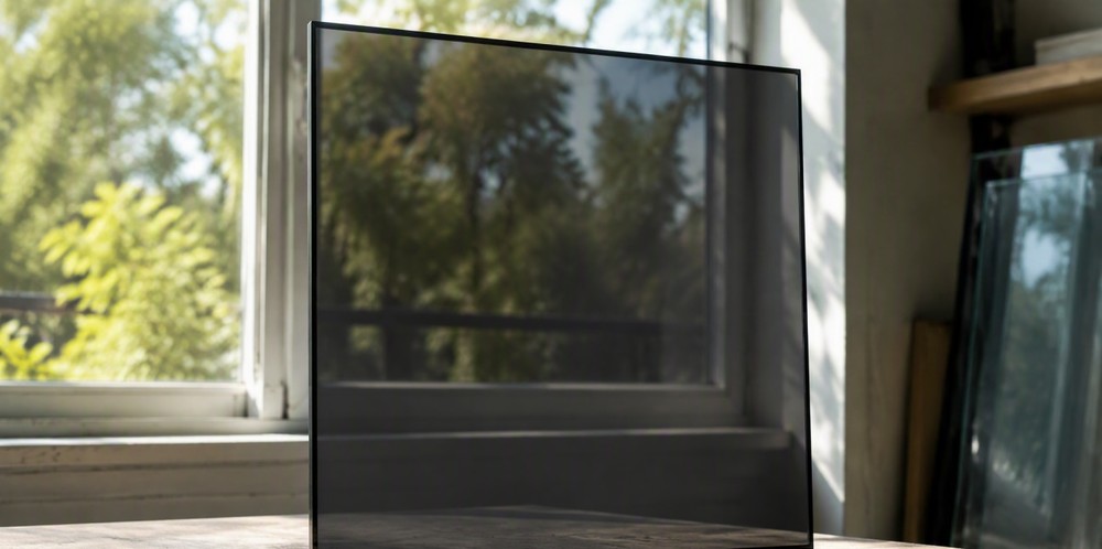 Semi-transparent thin-film photovoltaic glass.
Representative Products at a Glance
The products below cover most requests we receive. Thickness, doping, substrate, and dimensions are adjustable on every line.
| Product |
Material |
Typical Form |
Main Use |
| Silicon Sputtering Targets (Planar) |
5N silicon |
Bonded plates |
PVD thin-film deposition |
| Rotary Silicon Targets |
5N silicon |
Tubular targets |
Large-area coating lines |
| a-Si:H Coated Glass Substrates |
Intrinsic a-Si:H |
0.1–2 µm on glass |
Device research, PV labs |
| Doped a-Si:H Layers |
n-type / p-type a-Si:H |
On glass or TCO |
PIN / NIP structure research |
| µc-Si:H Films |
Microcrystalline silicon |
On glass, Raman-verified |
Tandem bottom-cell research |
| Thin-Film Silicon Test Coupons |
a-Si or µc-Si |
Small square coupons |
PECVD calibration, metrology |
| Flexible Thin-Film Silicon |
a-Si:H on polyimide |
Strips and sheets |
Flexible PV, wearable power R&D |
| Semi-Transparent a-Si Glass |
a-Si on TCO glass |
Adjustable transparency |
BIPV development |
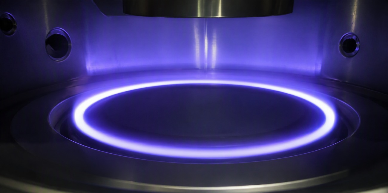 Plasma glowing over a silicon target during sputtering.
Quality and Characterization
Thin films live or die by parameters that are invisible to the eye, so every lot is measured before it ships. Film thickness is mapped across the substrate by ellipsometry or profilometry; microcrystalline material is verified by Raman spectroscopy for crystalline volume fraction; doped layers are checked for dark and photo conductivity; and sputtering targets are certified for purity and density, then bonded to their backing plates under controlled conditions. A data sheet with the measured values accompanies each shipment — the numbers your process engineer will ask for are already in the box.
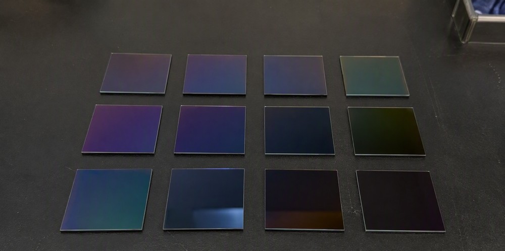 Thin-film silicon test coupons ready for shipment.
How to Specify Thin-Film Silicon Materials
- Start from the deposition route: running your own PVD line calls for targets; developing devices without a coater calls for ready-coated substrates.
- Define the film: amorphous or microcrystalline, intrinsic or doped, and the thickness window your structure requires.
- Name the substrate: soda-lime or borosilicate glass, TCO-coated glass, polyimide, or metal foil — plus the coated area.
- Say what you will measure: if the material feeds a published experiment, tell us which parameters matter and we will certify those specifically.
Many of our orders never appear in any catalog: targets machined to an unusual cathode geometry, coatings stacked to a specified PIN sequence, transparency tuned for a particular BIPV glazing concept, coupon sets prepared for a round-robin study between laboratories. Single research coupons and recurring production volumes are equally routine, and custom work carries the same measurement documentation as standard stock.
Describe the film, the substrate, and the experiment or product behind them — we will deposit or supply the thin-film silicon to match.
For Research or Industrial Raw Materials, Not For Personal Medical Use!