Every efficiency record in mainstream photovoltaics belongs to the same material. A monocrystalline silicon solar cell has passed 26.8% in the laboratory — a figure no multicrystalline device has ever approached — and the reason comes down to structure: one continuous crystal lattice from one end of the ingot to the other, with no grain boundaries to trap charge carriers on their way to the contacts.
Eata Silicon supplies monocrystalline silicon in the forms that cell producers, device engineers, and research laboratories actually buy: Czochralski-grown ingots and wafers for solar production, float-zone material for high-resistivity work, and prime or test substrates for device research. Check the product list below for availability, or read on for a guide to the options.
Browse Our Products
 Czochralski pullers on the crystal growth floor.
One Crystal, No Boundaries: Why Mono Wins
In a multicrystalline ingot, the lattice restarts at every grain — and every restart is a boundary where carriers recombine and efficiency bleeds away. Monocrystalline silicon sidesteps the problem entirely. Grown from a single oriented seed, the crystal carries one lattice orientation throughout, which translates directly into longer minority-carrier lifetimes, higher open-circuit voltages, and cells that convert more of the same sunlight into power.
That is why the industry's efficiency race is run exclusively on mono: PERC lines built on monocrystalline wafers routinely reach 22–24% cell efficiency, TOPCon and HJT architectures push beyond 24% in production, and module-level records now exceed 24%. Uniformity brings a second, quieter benefit — batch-to-batch consistency that keeps cell lines stable and yields predictable.
CZ or Float Zone? Two Ways to Grow a Single Crystal
Czochralski (CZ) growth melts polysilicon in a quartz crucible and pulls the crystal from the melt. It is the economical, high-volume route — diameters from one inch to 300 mm and beyond, excellent availability, and the workhorse behind essentially all solar wafers and most integrated circuits. The quartz contact does introduce oxygen into the crystal, which keeps resistivity in the moderate range.
Float-zone (FZ) growth needs no crucible at all: a narrow molten zone travels along a suspended polysilicon rod, refining as it goes. The result is the purest monocrystalline silicon available — oxygen levels two orders of magnitude below CZ, and resistivities that can exceed 100,000 Ω·cm. Power semiconductors, particle detectors, and demanding research programs rely on it. We supply both routes and can advise which fits your device or cell design.
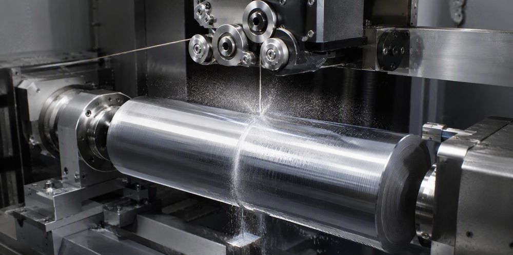 Squaring: from round ingot to rectangular brick.
From Ingot to Wafer
- Cropping: the ingot's crown and tail, where dopant segregation concentrates, are removed and returned to the melt as recyclable feed.
- Squaring: the round ingot is ground or wire-sawn into the pseudo-square cross-section that maximizes wafer area inside a module.
- Slicing: diamond-wire saws cut wafers with kerf losses under 100 µm, reaching thicknesses of 130–170 µm for solar and far thinner for specialty work.
- Finishing: cleaning, etching, or polishing brings the surface to its specified condition — as-cut, textured, single-side polished, or double-side polished.
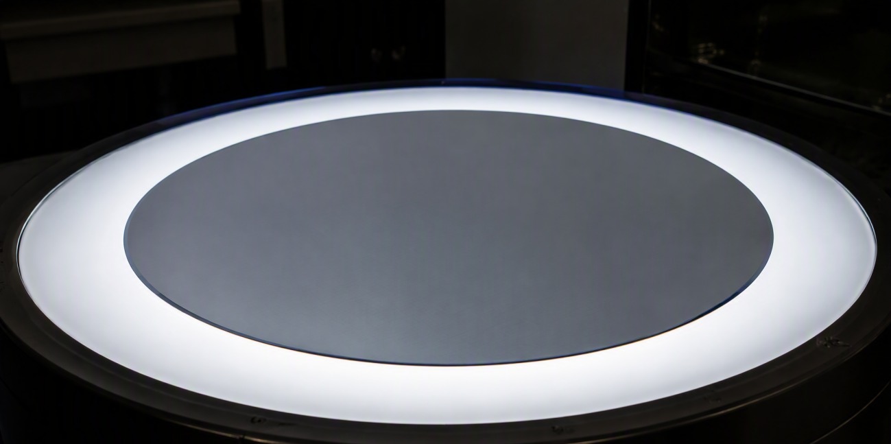
 A polished mono wafer — the cell maker's canvas.
p-type or n-type: Choosing a Doping Family
Boron-doped p-type wafers built the modern solar industry and still power most PERC production — proven, economical, and available at every mainstream size. The momentum, though, is shifting. n-type wafers, doped with phosphorus or gallium, carry higher carrier lifetimes and shrug off the boron-oxygen light-induced degradation that costs p-type cells early-life output; gallium-doped variants address LID directly. TOPCon and HJT lines are built almost entirely on n-type, and analysts expect n-type architectures to take the majority of global module shipments within the next few years.
We stock both families across 182 mm, 210 mm, and rectangular 182R/210R formats, with resistivity windows matched to your cell process rather than to a generic catalog entry.
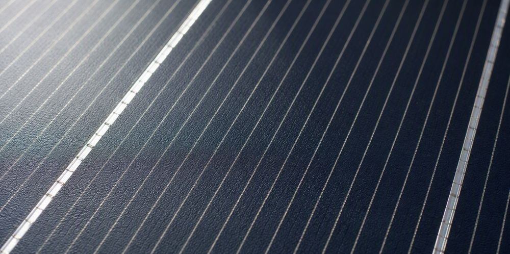 Fine gridlines on a finished monocrystalline cell.
Where Monocrystalline Silicon Performs
- Solar cell production: PERC on p-type, TOPCon and HJT on n-type — the substrate behind every leading cell architecture.
- Semiconductor and MEMS research: prime, test, and research-grade CZ wafers in 《100》, 《111》, and 《110》 orientations for device fabrication and process development.
- Power electronics: high-resistivity FZ silicon for IGBTs, thyristors, and diodes that switch serious power.
- Detectors and scientific instruments: ultra-pure FZ material where low oxygen and high resistivity are non-negotiable.
- Pilot and qualification lines: test-grade and reclaim wafers for equipment setup, training, and process trials at lower cost.
 Monocrystalline modules at work in the field.
Representative Products at a Glance
Our most requested monocrystalline products are listed below. Diameters, orientations, and resistivities outside the table can be sourced or grown to order.
| Product |
Growth / Doping |
Typical Specification |
Main Use |
| Solar-Grade Mono Silicon Ingots |
CZ |
200–300 mm diameter |
Wafer slicing for cell lines |
| p-type Mono Solar Wafers |
CZ, boron-doped |
182 / 210 mm, 130–170 µm |
PERC cell production |
| n-type Mono Solar Wafers |
CZ, P / Ga-doped |
182 / 210 mm, 130–170 µm |
TOPCon and HJT cells |
| Rectangular Mono Wafers |
CZ |
182R / 210R formats |
High-density module layouts |
| FZ Monocrystalline Silicon |
Float zone |
High resistivity, ultra-low oxygen |
Power devices, detectors |
| Prime / Test Silicon Wafers |
CZ / FZ |
《100》, 《111》, SSP / DSP |
Semiconductor research, MEMS |
| Reclaim & Test-Grade Wafers |
CZ |
Solar / electronic grade |
Pilot lines, tool qualification |
 Every wafer passes inspection before packing.
How to Specify Monocrystalline Silicon
- Solar cell lines: name the architecture first — PERC, TOPCon, or HJT — then wafer size, thickness, and resistivity window; doping family follows from there.
- Research substrates: give us orientation, diameter, thickness, polish (SSP or DSP), and resistivity; CZ covers most work, FZ covers the demanding rest.
- Power device programs: specify target resistivity and tolerance — float-zone gas-phase doping holds remarkably uniform values along the full crystal length.
- Uncertain on trade-offs? share the device or cell design and we will recommend the most economical grade that meets it.
Custom Monocrystalline Silicon Services
Off-standard requests are routine here: custom resistivity bands and dopants, non-standard wafer diameters and thicknesses, specific crystal orientations, thin wafers for tandem and flexible-cell research, and small-lot FZ material for instrument builders. Orders scale from a single research wafer to recurring pallet volumes, each lot documented with the certificates your quality system expects.
Tell us the specification your design calls for — we will grow, slice, or source the monocrystalline silicon to match it.
For Research or Industrial Raw Materials, Not For Personal Medical Use!