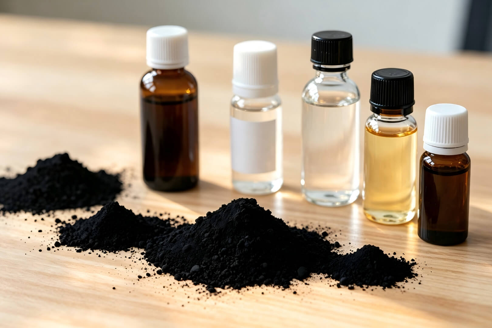
Between quartz rock and a finished solar panel sits the purest material most industries will ever handle. Metallurgical silicon leaves the arc furnace at 98–99% purity; polycrystalline silicon — polysilicon — begins where that stops, at six nines (99.9999%), and runs as high as eleven nines for semiconductor work. It is the feedstock from which virtually every solar wafer and silicon chip on earth is grown, and roughly 97.6% of world output flows into photovoltaics alone.
Eata Silicon supplies polysilicon in the physical forms crystal growers actually charge: crushed Siemens-process chunks, cut rod segments, and free-flowing FBR granules, graded from cost-effective multi-grade material up to 11N electronic grade.
Browse Our Products
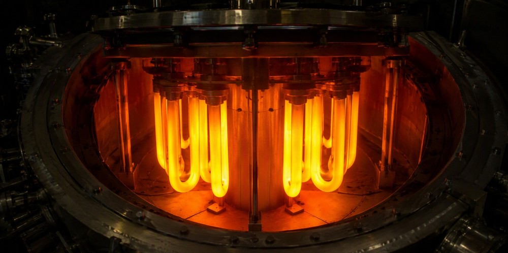 Slim rods glowing inside a Siemens bell-jar reactor.
What Polycrystalline Silicon Actually Is
The name confuses many first-time buyers, so it is worth being precise. Polycrystalline silicon is hyper-pure silicon produced by chemical vapor deposition: silicon atoms arrive from a gas phase and stack onto a heated starter rod, building a solid mass made of countless tiny interlocked grains. That grain structure is what the "poly" refers to — and it is only temporary. The moment the material is remelted in a crystal grower's crucible, the grains disappear, and the silicon is regrown as a single-crystal ingot or cast as a multicrystalline block.
In other words, polysilicon is not a wafer material but the refined feedstock upstream of one — the industry's standardized way of moving purity from the refinery to the furnace. The volumes involved are striking: producing one megawatt of photovoltaic capacity consumes about seven tonnes of polysilicon, which is why solar demand now dwarfs every other use.
How the Siemens Process Makes It
More than nine out of every ten kilograms of polysilicon sold today come from the Siemens process, a route refined continuously since the 1950s. Four linked steps turn 98% metallurgical silicon into material pure enough for semiconductors:
- Chlorosilane synthesis: ground metallurgical silicon reacts with hydrogen chloride in a fluidized bed at around 300 °C, forming trichlorosilane (TCS) — a volatile liquid that carries the silicon but leaves most impurities behind.
- Fractional distillation: TCS boils at just 31.8 °C, so tall multi-stage distillation columns strip out contaminant chlorides again and again, until the liquid is purer than virtually any industrial chemical.
- Chemical vapor deposition: the purified TCS, mixed with hydrogen, decomposes inside a steel bell-jar reactor onto U-shaped silicon slim rods electrically heated to roughly 1,100–1,150 °C. Over several days the rods swell from about 20 mm starters to 150–180 mm finished diameter.
- Closing the loop: off-gas hydrogen and HCl are recovered and reused, while the silicon tetrachloride by-product is converted back into TCS through hydrochlorination — so almost nothing leaves the plant except product.
The harvested rods are then crushed in cleanrooms into the chunks that fill crucibles. The process is energy-hungry, yet relentless engineering has pushed leading producers' cash costs below US$10 per kilogram. A complementary route, the fluidized bed reactor (FBR), grows free-flowing granules on seed particles with about one-tenth of a rod reactor's electricity; blending granules fifty-fifty with chunks can cut crucible filling time by roughly 40% and raise charge weight by about 30%.
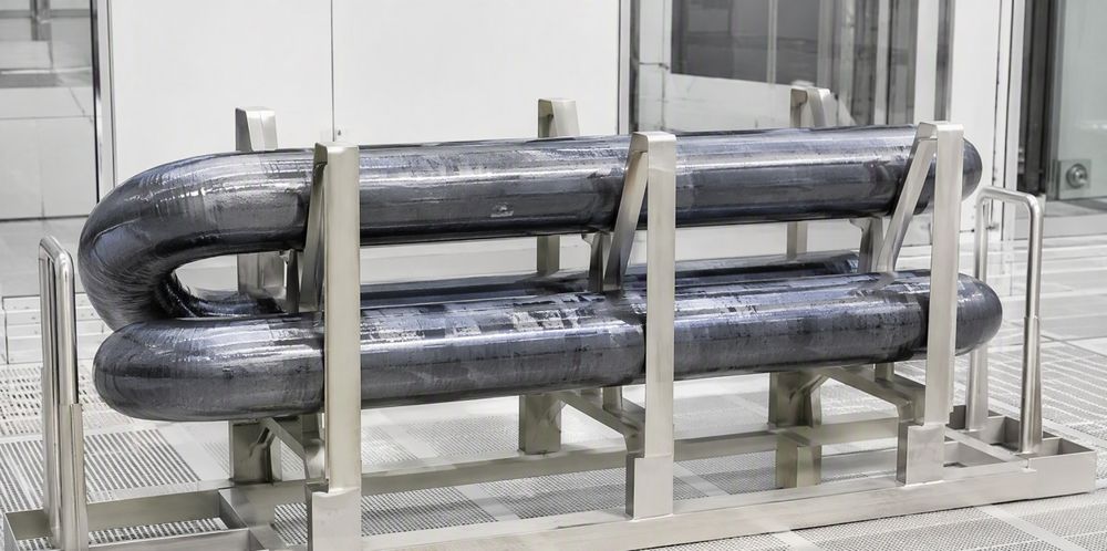 A harvested U-shaped rod pair fresh from the reactor.
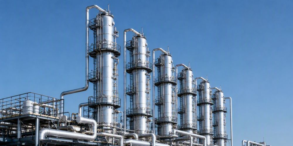 Tall columns where trichlorosilane is purified to electronic quality.
Picking a Purity: Solar Grade vs. Electronic Grade
Purity is the axis on which the entire polysilicon market turns. Deeper TCS distillation and post-harvest surface etching buy additional "nines," and each tier serves a different furnace:
| Grade Tier |
Typical Purity |
Typical Destination |
| Solar Multi-Grade |
7N–8N (99.99999–99.999999%) |
Multicrystalline ingot casting |
| Solar Mono-Grade |
9N–10N (99.9999999–99.99999999%) |
CZ pulling for monocrystalline wafers |
| Electronic Grade |
10N–11N and above |
Semiconductor crystal growth, float-zone feedstock |
Where the Material Goes
- Monocrystalline ingot pulling: the dominant use — chunks and granules melted in quartz crucibles and grown into CZ single crystals for solar wafers.
- Multicrystalline casting: multi-grade feedstock directionally solidified into large cast bricks for wafer slicing.
- Continuous Czochralski (CCz) lines: free-flowing FBR granules that recharge the melt without stopping the pull.
- Float-zone feedstock: straight rod sections refined into the ultra-high-resistivity crystals behind power semiconductors and detectors.
- Semiconductor crystal growth: 11N-class electronic-grade chunks for the ingots that become integrated-circuit wafers.
- n-type cell programs: low-donor, low-boron feedstock for TOPCon and HJT ingots where every fraction of a ppb matters.
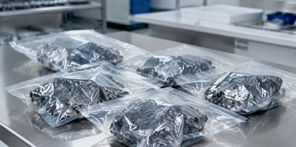 Cleanroom-packed chunks in double polyethylene bags.
Representative Products at a Glance
The grades and forms below cover the bulk of what our customers order. Chunk size windows, purity targets, and packaging can all be adjusted on request.
| Product |
Route / Grade |
Typical Form |
Main Use |
| Solar-Grade Chunks (Multi) |
Siemens, 7N–8N |
Crushed chunks, sized |
Multicrystalline casting |
| Mono-Grade Chunks |
Siemens, 9N–10N |
Chunks, surface-etched |
CZ mono ingot pulling |
| Electronic-Grade Polysilicon |
Siemens, 10N–11N |
Chunks or rod sections |
Semiconductor crystal growth |
| Polysilicon Rod Segments |
Siemens |
Cut rod lengths |
Float-zone feedstock, specialty melts |
| FBR Granular Polysilicon |
Fluidized bed, 6N–9N |
Free-flowing granules |
Crucible recharge, CCz lines |
| n-type Low-Donor Feedstock |
Siemens, tight B/P limits |
Chunks |
TOPCon and HJT ingot growth |
| Recharge & Secondary Material |
Solar grade |
Tails, popcorn, fines |
Blending and recharge melts |
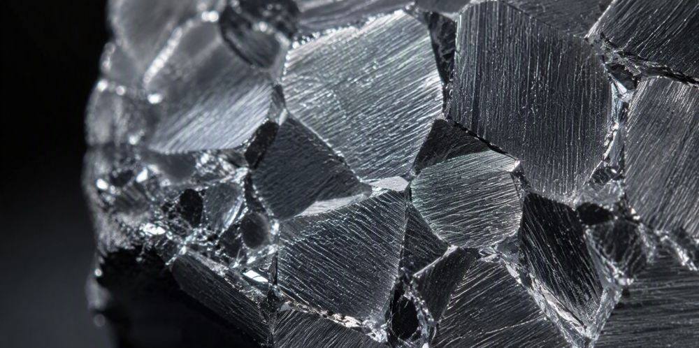 Faceted grain structure of as-grown polysilicon.
Quality Control and Packaging
Purity achieved in the reactor means little if it is lost on the packing line, so every downstream step happens under cleanroom discipline. Rods are crushed and classified on contamination-controlled equipment, optionally surface-etched to remove handling residues, then sealed in double polyethylene bags before entering drums or cartons. Lots ship with a certificate of analysis covering donor and acceptor concentrations, total bulk and surface metals, carbon, and oxygen — with resistivity and lifetime data added for solar mono-grade and electronic-grade material. Full batch traceability comes standard, from reactor run to bag label.
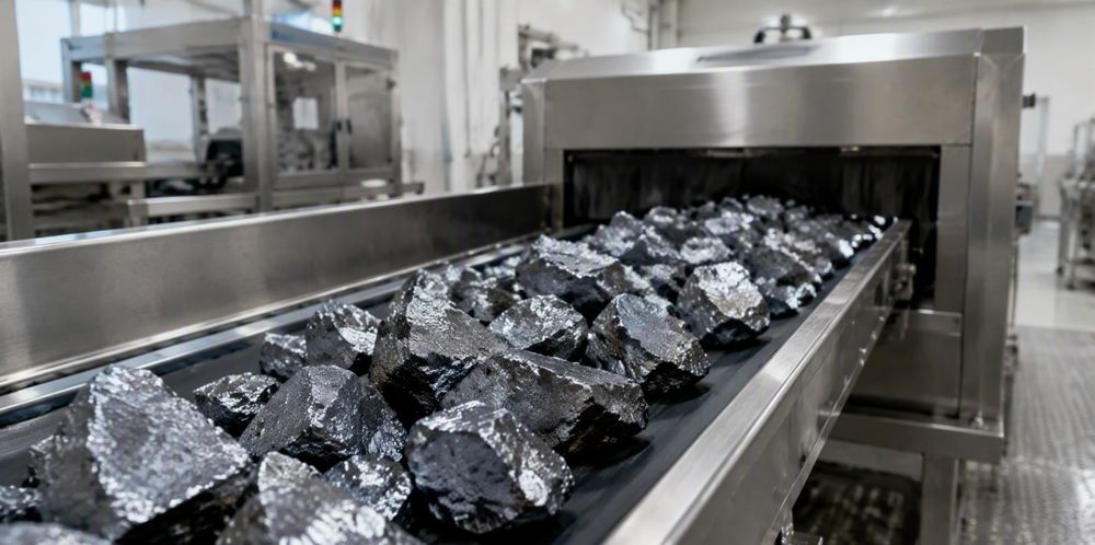 Chunk sorting and inspection before final packing.
How to Choose the Right Polysilicon
- Let the cell architecture set the grade: multicrystalline casting runs economically on 7N–8N; PERC lines prefer 9N; TOPCon and HJT programs should insist on low-donor 9N–10N material.
- Match the form to the furnace: chunks for standard crucible charges, granules where recharge speed and packing density count, or a specified chunk–granule blend for the best of both.
- Semiconductor work needs paper as much as purity: for electronic grade, verify the full impurity panel and lot traceability, not just the headline "11N."
- Buying on price alone? remember that off-spec feedstock costs far more in lost crystals and downtime than it saves per kilogram.
Custom Polycrystalline Silicon Services
Standard grades cover most furnaces — and for the rest, we build to order. Chunk size windows can be tightened to your charging method; chunk–granule blends can be pre-mixed to your specified ratio; donor, acceptor, carbon, and metals limits can be narrowed for demanding n-type or electronic-grade programs; and packaging can be adapted from small research quantities to full container lots, always with the certificates your quality system requires.
Send us your target specification — purity, form, size window, and quantity — and we will match a polysilicon supply to your furnace.
For Research or Industrial Raw Materials, Not For Personal Medical Use!