Roughly nineteen out of every twenty solar modules made today still start from crystalline silicon — and the material decisions taken at the very start of that chain echo all the way into module efficiency, degradation behavior, and cost per watt. Feedstock purity shapes ingot quality. Crystal structure shapes cell architecture. Wafer geometry shapes factory throughput.
Eata Silicon works across that entire chain with four product families: Monocrystalline Silicon, Polycrystalline Silicon, Photovoltaic Silicon Wafers, and Thin-Film Silicon Materials. The list below shows what is currently available; further down, each family gets a closer look.
Browse Our Products
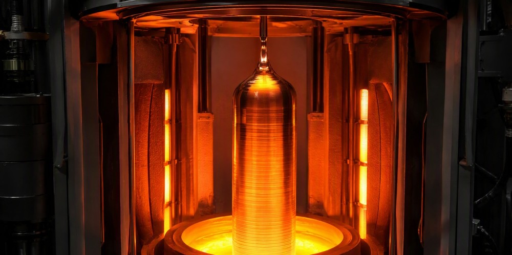 Crystal pulling: where monocrystalline silicon begins.
The Czochralski method grows the industry's benchmark material. Solar-grade polysilicon at 6N purity or better melts in a quartz crucible at around 1,414 °C; a seed crystal touches the melt, then rotates and withdraws at a carefully controlled one to two millimeters per minute. Silicon atoms latch on in the seed's exact orientation, building a dislocation-free cylindrical ingot — typically 200 to 300 mm in diameter and up to two meters long — over a day or more of continuous growth.
That structural perfection is why every high-efficiency cell architecture — PERC, TOPCon, and HJT alike — is built on monocrystalline wafers. We supply mono material in both doping families: p-type for mainstream production and n-type (phosphorus- or gallium-doped) for premium TOPCon and HJT lines where higher minority-carrier lifetimes pay for themselves.
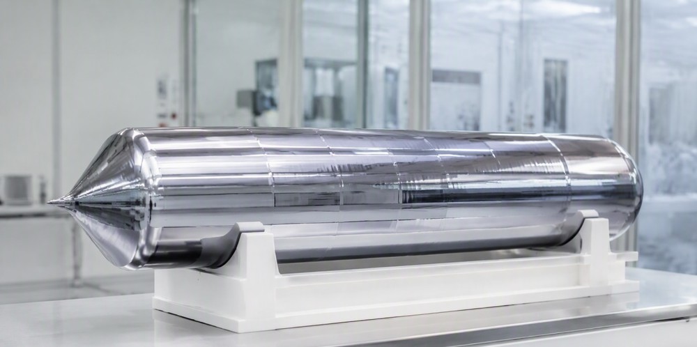 A finished single-crystal ingot ready for cropping and squaring.
Casting takes a different route to the same destination. Molten silicon is poured into a square crucible and solidified directionally from the bottom up, producing a block whose surface shows the telltale mosaic of crystal grains. The process is faster and less energy-hungry than crystal pulling, and the square geometry eliminates the corner-trimming losses that cylindrical ingots suffer on the way to wafers.
Grain boundaries do cost some conversion efficiency compared with mono, but for cost-sensitive cell lines, ground-mount projects with generous space, and feedstock blending, cast multicrystalline silicon remains a rational choice. High-performance casting with seeded, finer grains narrows the gap further.
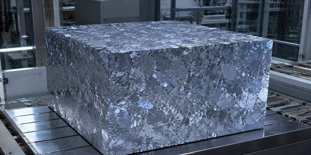 Cast multicrystalline brick with its signature grain mosaic.
Between ingot and cell sits the wafer — the format the cell line actually buys. Standard formats have migrated from 156.75 mm up to 182 mm and 210 mm, with rectangular 182R and 210R variants squeezing more watts into the same module outline. Meanwhile diamond-wire sawing has pushed kerf loss under 100 micrometers and pulled typical wafer thickness down toward the 130–170 µm window, stretching every kilogram of silicon further.
We offer mono wafers in p-type and n-type across the mainstream sizes, multicrystalline wafers for cost-driven lines, and custom thicknesses for research programs. Surface options range from as-cut through textured and cleaned, ready for diffusion or passivation.
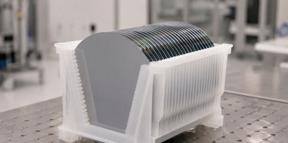 Sawn and cleaned wafers stacked for the cell line.
Thin-film silicon plays by different rules. Instead of growing and slicing crystals, plasma-enhanced chemical vapor deposition builds hydrogenated amorphous silicon (a-Si:H) directly onto glass or flexible substrates at around 200 °C — a working layer of one to two micrometers where a wafer needs well over a hundred. The payoff: strong low-light and diffuse-light response, a gentler temperature coefficient, semi-transparency options, and form factors that crystalline modules simply cannot match, from curved surfaces to building-integrated glass.
Stacking a microcrystalline silicon bottom cell beneath the amorphous top cell creates the micromorph tandem, which harvests a wider slice of the spectrum and reaches stabilized efficiencies around 11–12%. Amorphous silicon also hides inside today's most efficient crystalline cells, where ultra-thin a-Si layers passivate HJT contacts. We supply deposition-grade materials and substrates for both module production and laboratory coating work.
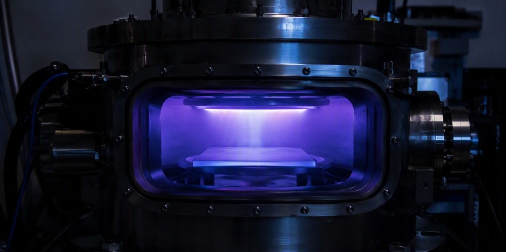 Plasma deposition builds thin-film silicon layer by layer.
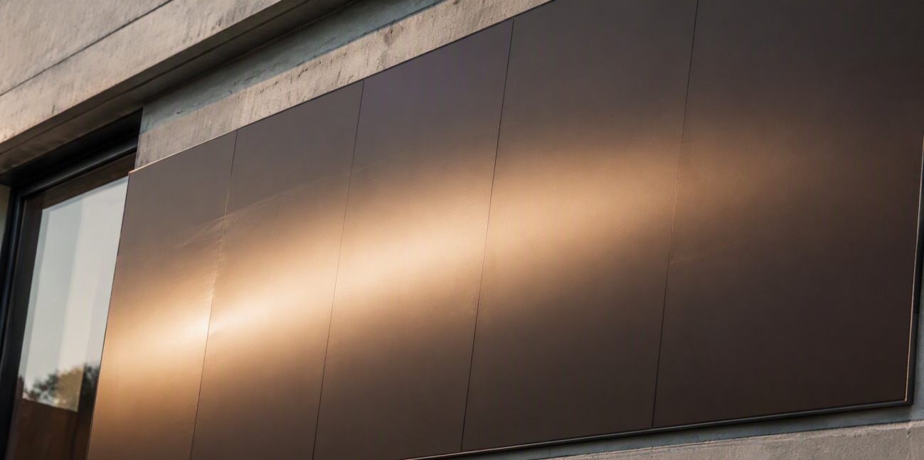 Thin-film silicon on glass, integrated into a facade.
Representative Products at a Glance
The range below covers what PV buyers request most often. If your specification falls outside it — an unusual wafer geometry, a deposition-grade material with tight hydrogen content — ask anyway; that is where our sourcing team does its best work.
| Product |
Category |
Typical Specification |
Main Use |
| Solar-Grade Polysilicon Chunks |
Feedstock |
≥6N purity |
CZ pulling, crucible recharge |
| Granular Solar Silicon |
Feedstock |
≥6N purity |
Continuous charging, FBR lines |
| Monocrystalline Silicon Ingots |
Monocrystalline Silicon |
200–300 mm diameter |
High-efficiency cell production |
| Mono Wafers, p-type / n-type |
Photovoltaic Silicon Wafers |
182 / 210 mm, 130–170 µm |
PERC, TOPCon, HJT cell lines |
| Multicrystalline Wafers |
Photovoltaic Silicon Wafers |
156.75 mm and larger |
Cost-driven cell production |
| Amorphous Silicon Materials (a-Si:H) |
Thin-Film Silicon |
Deposition grade |
Thin-film modules, HJT passivation |
| Microcrystalline Silicon Materials (µc-Si:H) |
Thin-Film Silicon |
Deposition grade |
Micromorph tandem research |
| High-Purity Quartz Crucibles |
Consumables |
Solar grade |
CZ and casting furnaces |
How to Specify Your PV Silicon
- Cell architecture first: PERC lines run well on p-type mono; TOPCon and HJT generally call for n-type wafers with tighter resistivity windows — share your target and we will match it.
- Feedstock for crystal growth: state purity, chunk or granular form, and your boron and phosphorus ceilings so furnace loads stay consistent from batch to batch.
- Wafer buyers: confirm format (182, 210, or rectangular), thickness, and surface condition — as-cut, textured, or cleaned.
- Thin-film and R&D: tell us your deposition platform and layer stack; we can align material purity and substrate preparation accordingly.
Custom Photovoltaic Material Services
Solar production rarely fits a catalog perfectly. Eata Silicon supports custom resistivity and dopant targets, non-standard wafer sizes and thicknesses, blended feedstock charges tuned to your furnace recipe, and laboratory quantities of thin-film materials for pilot coating lines. Whether the requirement is a single research ingot or a recurring container of wafers, we configure the material around your process rather than the other way around.
Tell us your cell technology and target specifications — we will put together the silicon that gets you there.
For Research or Industrial Raw Materials, Not For Personal Medical Use!