More than 90% of the world's solar cells are made from crystalline silicon, and every one of them begins life as a wafer. Long before a cell architecture adds its passivation layers and contacts, the wafer itself has already set the ceiling on performance: its crystal quality, resistivity, thickness, and surface condition decide how much of the sun a finished module can harvest. That is why cell producers increasingly treat wafer sourcing as a strategic decision rather than a commodity purchase.
Eata Silicon supplies photovoltaic silicon wafers across the formats and doping families the industry runs on today — p-type for PERC, n-type for TOPCon and HJT, in 182 mm, 210 mm, and the fast-growing rectangular variants.
Browse Our Products
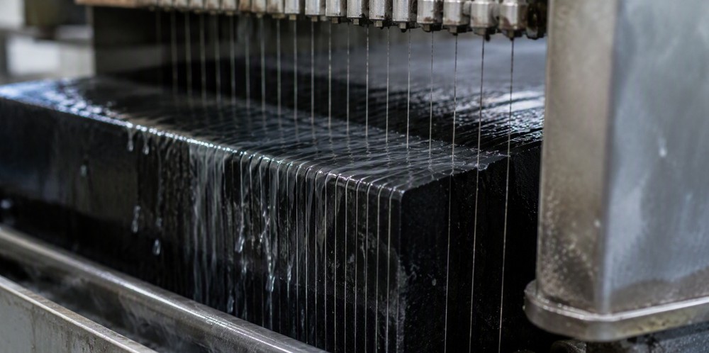 A diamond-wire web slicing a silicon brick into wafers.
From Brick to Wafer: How Slicing Sets Quality
A wafer's fate is largely decided at the saw. After the grown ingot is squared into bricks, a web of diamond-coated wires — today with steel cores as fine as 36–45 µm — travels at 10–20 m/s and slices the brick into hundreds of wafers in a single pass. The shift from loose-abrasive slurry sawing to fixed diamond wire transformed the economics: kerf loss per cut fell from roughly 100–150 µm to 60–80 µm, subsurface damage halved to 5–15 µm, and total thickness variation can now be held within about 10 µm. Considering that older lines once lost close to 40% of the silicon as kerf powder, these gains translate directly into more watts from every kilogram of polysilicon.
What leaves the saw is an as-cut wafer: uniform, low-damage, and ready either for the buyer's own texture line or for a pre-texturing step before shipment.
Formats: The 182, 210, and Rectangular Landscape
Wafer dimensions shape everything downstream — cell power, module layout, even shipping-container economics. The market has consolidated around two families, with rectangular hybrids bridging them. InfoLink figures show the 182-series and 210-series splitting the market roughly 70:30 in 2024, while the 210R rectangular format jumped from 19% to 28.7% of top-five cell shipments within a year and is expected to become the mainstream format.
| Format |
Dimensions |
Position in the Market |
| M10 (182) |
182 × 182 mm |
Long-running mainstream; vast installed cell-line base |
| 182R / 18X |
182.2 × 183.5–199 mm |
Near-rectangular variants; raised module power on existing lines |
| 210R |
182.2 × 210 mm |
Fastest-growing format; high-power modules, lower BOS cost |
| G12 (210) |
210 × 210 mm |
Maximum power per wafer; utility-scale module designs |
| M6 (166) and smaller |
166 × 166 mm and below |
Legacy sizes fading toward single-digit share |
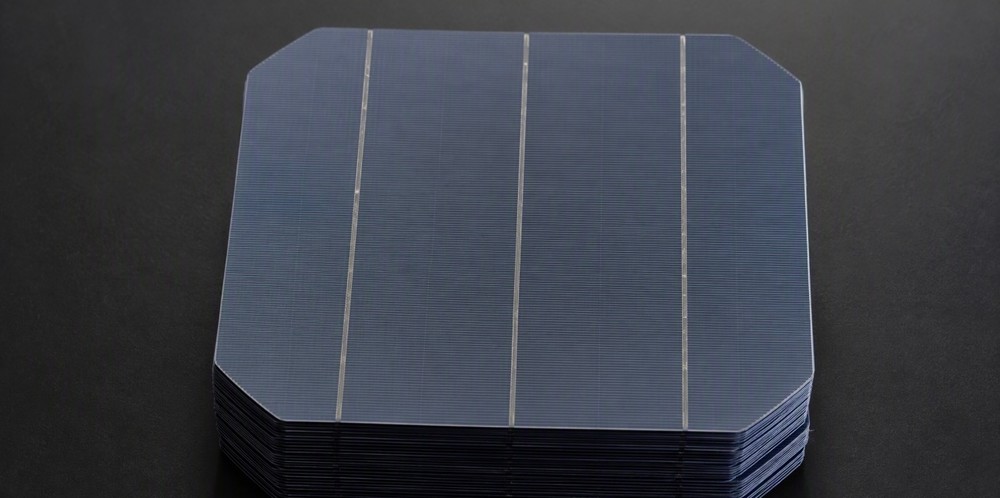 A stack of freshly sliced pseudo-square solar wafers.
p-type or n-type: Follow the Cell Architecture
The doping question answers itself once the cell line is named. PERC production runs on boron- or gallium-doped p-type wafers, typically 130–150 µm thick. TOPCon — which accounted for over 88% of top-five cell shipments in 2025 — is built on phosphorus-doped n-type wafers at 120–140 µm, prized for their long carrier lifetimes and freedom from boron-oxygen degradation. HJT lines push n-type thinner still, at 110–130 µm with resistivity commonly held in the 1–3 Ω·cm window, and pilot work has demonstrated wafers as thin as 90 µm at viable breakage rates.
Eata Silicon stocks both families across the mainstream formats, with resistivity windows matched to the target cell process — not to a generic catalog entry.
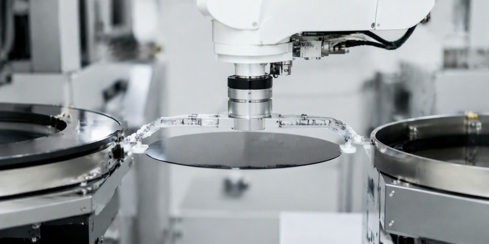 Automated wafer transfer between process stations.
Thinner Every Year: Why Thickness Matters
Every micrometer shaved from a wafer saves silicon, and at scale the arithmetic is compelling — moving from 150 µm toward 130 µm trims silicon consumption per watt by roughly 5–10%. The trade-off is mechanical: thinner wafers break more easily, so the move downward depends on saws that hold TTV tight, handling systems that treat wafers gently, and cell processes adapted to flexible substrates. Ultra-thin wafers in the 90–120 µm range are now standard requests from HJT lines and from perovskite-silicon tandem research programs, both of which we supply.
As-Cut or Pre-Textured: Surface Options
Raw as-cut wafers reflect too much light to make a good cell, so the industry textures them — anisotropic alkaline etching (KOH or NaOH) that sculpts the 《100》 surface into a field of random pyramids. Modern additive-controlled processes produce 1–2 µm pyramids with excellent uniformity, cutting reflectance to around 10% before the anti-reflection coating and below 3% on a finished cell. HJT and tandem work increasingly asks for finer, sub-micrometer textures that accept amorphous silicon layers smoothly. Buyers can order from us either way: as-cut wafers for in-house texturing, or pre-textured wafers ready to go straight into diffusion.
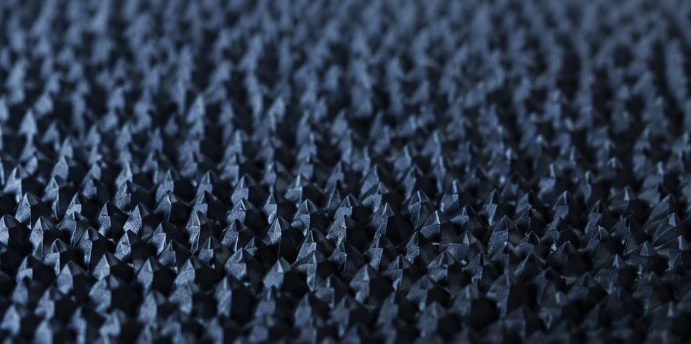 Random pyramid texture on a monocrystalline wafer surface.
Representative Products at a Glance
The wafers below cover the bulk of current demand. Thickness, resistivity, and surface condition can be tuned on any of them — and formats beyond the table can be sliced to order.
| Product |
Type / Format |
Typical Specification |
Main Use |
| p-type PERC Solar Wafers |
p-type, 182 mm |
130–150 µm, B / Ga-doped |
PERC cell production |
| n-type TOPCon Wafers |
n-type, 182 mm |
120–140 µm, P-doped |
TOPCon cell lines |
| 210R Rectangular Wafers |
n-type, 182.2×210 mm |
130 µm |
High-power TOPCon modules |
| HJT-Ready Wafers |
n-type, 210 mm |
110–130 µm, 1–3 Ω·cm |
Heterojunction cell lines |
| 182R Rectangular Wafers |
p / n-type, 182.2×183.75 mm |
130–150 µm |
High-density module layouts |
| Pre-Textured Wafers |
mono, alkaline pyramid |
1–2 µm texture, ~10% reflectance |
Direct-to-diffusion processing |
| Ultra-Thin Research Wafers |
n-type, custom formats |
90–120 µm |
Tandem, flexible, HJT R&D |
| Test & Reclaim Wafers |
solar grade |
As-cut or textured |
Pilot lines, tool qualification |
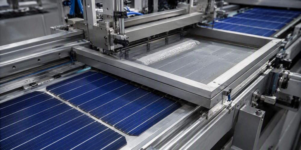 Wafers become cells on the metallization line.
Inspection and Packing Standards
A wafer is only as valuable as its survival rate through your line, so outgoing lots are screened accordingly: automated optical inspection for cracks, chips, and edge defects; thickness and TTV mapping; resistivity verification against the ordered window; and minority-carrier lifetime sampling on n-type lots. Approved wafers are shrink-wrapped in stacks, cushioned in foam-lined boxes with moisture protection, and shipped with lot documentation covering dimensions, thickness, resistivity, and doping — traceable back to the ingot.
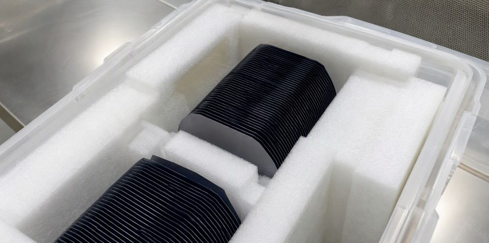 Foam-cushioned wafer stacks ready for shipment.
How to Specify Your Wafer Order
- Name the cell architecture first: PERC, TOPCon, HJT, or tandem research — doping family, thickness, and resistivity all follow from it.
- Fix the format and thickness: 182 mm, 210R, 210 mm, or a legacy size for an existing line; 150 µm down to 90 µm depending on process maturity.
- Choose the surface: as-cut for in-house texturing, or pre-textured with standard or fine pyramids to skip a wet step.
- State the resistivity window: tight windows cost a little more per wafer and repay it in line stability and binning yield.
Custom Photovoltaic Silicon Wafer Services
Beyond standard formats, we routinely handle non-catalog requests: unusual thicknesses for tandem and flexible-cell research, custom resistivity bands and dopants, fine or sub-micrometer texturing, mixed-format consignments for multi-line plants, and small development lots alongside volume supply. Every custom lot ships with the same inspection data and traceability as our standard products.
Share your cell process and target specification with us — we will cut, texture, and document the wafers to fit it.
For Research or Industrial Raw Materials, Not For Personal Medical Use!